Instant Connection for Pixel Streaming
— New Feature Automated Setup

How to Use KiCad With Claude: MCP & Computer Use Guide Meta
Architecture
-
How to Use KiCad With Claude: MCP & Computer Use Guide Meta
Architecture
How to Use KiCad With Claude: MCP & Computer Use Guide Meta
Architecture
-
Table of Contents
A sensor board can pass its rule checks and still arrive with a connector facing the wrong direction. The schematic may be consistent, the copper clearances acceptable, and the manufacturing files complete, yet the selected footprint might not match the part you ordered. Using Claude with KiCad is most useful when it helps you investigate those gaps, not just generate a circuit that looks plausible.
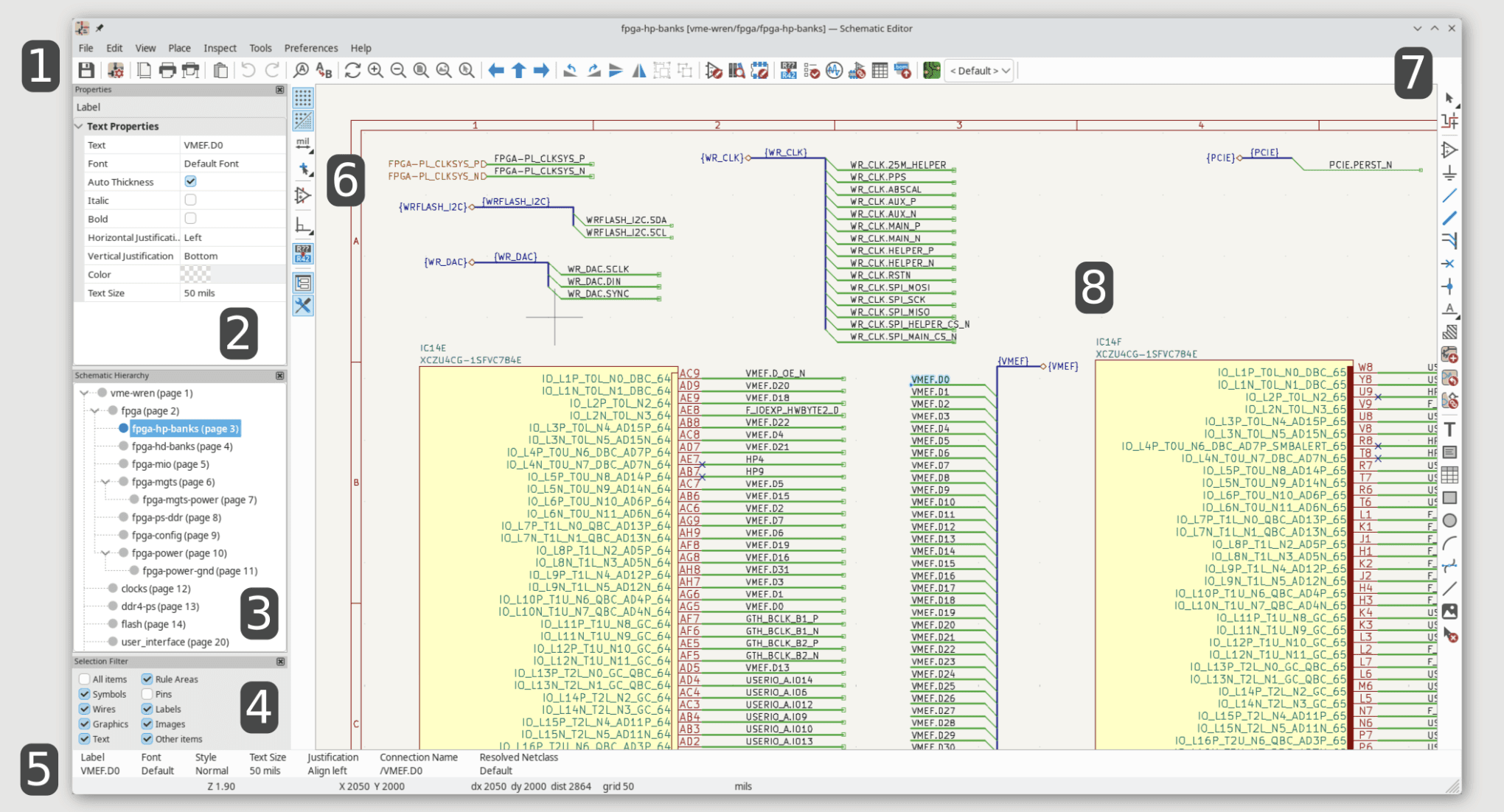
There are two complementary ways to connect that assistance to your project. A community-built MCP connector can expose design information and supported editing operations to Claude. Depending on its implementation, those tools may read saved files, invoke KiCad utilities, or interact with the running PCB Editor. Claude’s Computer Use provides a different route: working through the application interface to inspect dialogs, navigate findings, and perform visual checks.
Neither approach gives Claude unrestricted understanding of your hardware. Access depends on your KiCad version, connector, Claude environment, and permissions. A successful operation also needs verification against the correct project state.
This guide follows an existing two-layer sensor board through review, a controlled placement change, and manufacturing output checks. The goal is practical assistance with traceable changes, while you retain responsibility for electrical decisions and production approval.
Source: KiCad Documentation Contributors
Choose the Right Kind of Access for Each KiCad Task
Before connecting Claude, decide what the task actually requires. Reading a component list, moving a footprint, and inspecting a connector in the 3D Viewer are different operations. They do not necessarily need the same access method.
Access method | Best suited to | Main limitation |
|---|---|---|
Saved files and CLI | Project analysis, rule checks, manufacturing exports | May not reflect unsaved editor changes |
MCP connector | Structured queries and supported design operations | Capabilities depend on the connector and backend |
Computer Use | Dialogs, visual inspection, and interface interactions | Screen access does not provide complete design data |
These methods can overlap. An MCP server might invoke the KiCad CLI to run DRC, parse schematic files to inspect connections, and use an API for PCB operations. MCP describes how Claude accesses tools, not how those tools access KiCad.
That distinction matters for version compatibility. The official KiCad IPC API supports the running PCB Editor in KiCad 9 and 10. A connector that edits schematics in those versions must use another mechanism. Its schematic capabilities should not be assumed from its PCB capabilities.
For our sensor board, structured tools are useful for identifying references, nets, and footprint assignments. Computer Use can then help navigate the corresponding objects and examine their visual context.
Before either route makes changes, establish which project and revision Claude is inspecting. Ask whether each tool reads the saved file, the running editor, or its own in-memory copy. Otherwise, a successful check could describe an older board rather than the one visible on your screen.
Connect Claude to KiCad Without Mixing Backends
For a concrete starting point, the community-built KiCAD-MCP-Server provides a Python and TypeScript bridge between an MCP client and KiCad. It is not a native Claude integration or an official KiCad feature. Review its installation requirements and permissions before giving it access to a working design.
Install the connector and check its Python environment
The repository’s quick start specifies KiCad 9.0 or later, Node.js 18 or later, and Python 3.11 or later. It recommends the stable branch rather than unreleased changes on main:
These commands download and build the server, but they do not complete every platform-specific dependency step.
The important Python requirement is access to KiCad’s pcbnew module. An unrelated Python installation may run normally while failing to import it. Follow the connector’s platform guide for dependency installation, interpreter selection, and library paths. Windows and macOS installations can use KiCad’s bundled Python; Linux configuration depends on the installed packages.
Use paths detected on your machine. Do not copy a KiCad 9 library path into a KiCad 10 installation simply because it appears in an example.
Register the server with Claude
The connector’s Claude Desktop configuration launches the built server through Node. Its basic structure looks like this:
{
  "mcpServers": {
    "kicad": {
      "command": "node",
      "args": [
        "/ABSOLUTE/PATH/KiCAD-MCP-Server/dist/index.js"
      ]
{
  "mcpServers": {
    "kicad": {
      "command": "node",
      "args": [
        "/ABSOLUTE/PATH/KiCAD-MCP-Server/dist/index.js"
      ]
This is a template, not a complete cross-platform configuration. Replace the placeholders and include any additional environment settings required by your installation. Merge the entry with existing MCP settings instead of replacing other servers.
After restarting Claude Desktop, check that the server connects and exposes tools. If it fails, inspect the connection logs before asking Claude to troubleshoot through repeated design operations.
Start with a read-only project check
Use a copy of the sensor-board project for the first test:
Identify the KiCad project you can access. Report its project path, board file, schematic files, and component references. Explain whether the information comes from saved files or a running editor. Do not modify or save anything.
Compare the response with KiCad before proceeding. A connected server pointing to the wrong project is still the wrong setup.
Finally, treat live access as a separate capability. This connector documents its IPC-based UI integration as experimental. File-based tools do not necessarily require an open editor; live tools do. Confirm the backend and synchronization behavior of the specific operation you intend to use before enabling edits.
Review the Circuit Before Moving Components
Start with a question about the design, not an instruction to rearrange it. For our sensor board, the first question is whether the external connector connects the intended signals to the correct physical pins.
Ask Claude to extract the connector’s reference, symbol pin numbers, connected nets, assigned footprint, and manufacturer part number. If the connector cannot expose one of those details, supply the relevant file or inspect it in KiCad. Missing information should remain an explicit uncertainty.

Source: KiCad Documentation Contributors
Compare the symbol, footprint, and actual part
KiCad matches symbol pins to footprint pads by their numbers. A net connected to symbol pin 1 therefore needs to reach the appropriately numbered footprint pad. But that correspondence alone does not establish that the footprint represents your purchased connector.
Compare three sources: the schematic symbol, the assigned footprint, and the manufacturer’s datasheet for the exact part. Check pad numbering, pitch, mounting style, and the viewing direction used in the mechanical drawing. A mating-face drawing and a board-side view can make the same connector appear reversed.
A focused request would be:
Review J1 without changing the project. Compare its symbol pin numbers, connected nets, and footprint pad numbers against the supplied manufacturer datasheet. Identify the drawing’s viewing direction. Separate confirmed matches, suspected mismatches, and details you cannot verify.
Require datasheet page references for conclusions based on the document. If the part number is incomplete or the drawing is ambiguous, Claude should ask for clarification rather than choose an orientation.
Extend the review to the surrounding circuit
Once J1 is understood, examine the paths connected to it. For a sensor interface, that could include the supply rail, ground connection, signal lines, and any pull-up or protection components. Ask Claude to distinguish what the project explicitly records from what it infers about the intended operation.

Source: KiCad Documentation Contributors
A compact findings table keeps this review actionable:
Item | Evidence to compare | Required outcome |
|---|---|---|
Connector mapping | Nets, pin numbers, pad numbers, datasheet | Confirmed mapping or unresolved discrepancy |
Footprint selection | Exact package, pitch, mounting dimensions | Compatibility evidence |
Component identity | Value, part number, BOM fields | Missing or inconsistent information flagged |
Run ERC as a baseline, but do not turn this review into automatic warning suppression. Record each finding with its reference and supporting evidence.
The result should be a prioritized review, not an edited board. Resolve identity and connectivity questions before approving a placement change, because moving the wrong footprint more neatly does not fix the underlying design.
Make One PCB Change You Can Verify
With J1’s identity and pin mapping confirmed, the next task is a bounded placement change. Avoid asking Claude to “optimize the board.” That instruction leaves too much room to move components, alter routing, or change constraints without a clear acceptance test.
Instead, identify the footprint by reference and, where available, its unique identifier. Ask Claude to report its current position, rotation, board side, and lock status before proposing a change. Coordinates need units and a stated origin; rotation needs a clear absolute target rather than an ambiguous instruction such as “turn it around.”

Source: KiCad Documentation Contributors
Define the change before approving it
For our sensor board, the objective is to orient J1 toward the intended cable-entry edge without changing its electrical mapping. Claude should first inspect the surrounding area and explain whether the proposed placement would affect nearby components or existing copper.
A suitable request is:
Inspect J1 and propose a placement that faces the approved cable-entry edge. Report its current and proposed coordinates, rotation, board side, and expected routing impact. Preserve the footprint assignment, pad net assignments, board outline, mounting holes, and other components. Do not apply the change until I approve the exact placement.
Before approval, save a recoverable project copy. Establish which application or tool owns the editable state so that a later save from another instance does not overwrite the result. If J1 is locked, ask why before authorizing an override.
Once the proposal is acceptable, approve only that operation. If the connector cannot perform it reliably, stop or explicitly switch to an interface-based method.
Treat placement and routing as separate operations
A footprint can retain its pad net assignments while losing physical copper connections after movement. A successful position update therefore does not prove that the board remains connected.
KiCad’s interactive routing has its own behavior and settings. Do not assume a connector’s coordinate-editing tool behaves like dragging through the router. Ask Claude to report disconnected pads and affected tracks rather than silently launching a broader rerouting operation.
After the change, request a compact comparison:
Property | Verification |
|---|---|
Position and rotation | Match the approved target |
Footprint and board side | Remain unchanged |
Pad net assignments | Match the original mapping |
Surrounding objects | No unintended modifications |
Copper connections | Inspected for required repairs |
Read these properties back from the updated state instead of relying only on the tool’s success message. Inspect J1 in KiCad, then run the appropriate checks on the synchronized, saved revision. Any routing repair should become a separate, explicitly scoped task.
Let Computer Use Handle the Checks That Need a Screen
MCP tools can report coordinates, net assignments, and rule violations, but some questions are easier to investigate inside KiCad. Which way does the connector opening face? Which objects surround a clearance marker? Does the footprint preview match the package drawing?
Claude’s Computer Use can help navigate those checks in a supported desktop environment with your permission. Enable the feature in the appropriate Claude application and approve the required access. Connecting an MCP server alone does not grant screen control.
The following are practical workflows to try, not guarantees that Claude will interpret every KiCad view correctly. Begin with inspection-only instructions and keep project-changing actions separately authorized.
Cross-probe the connector instead of searching twice
KiCad supports cross-probing between schematic symbols and PCB footprints, including corresponding pins and pads. Claude can use this interface to navigate from J1 in the schematic to its physical representation.
Ask it to select the relevant pin, inspect the corresponding pad, and report the visible net and numbering. This helps connect the earlier structured review to the actual objects on screen.
Select J1 in the schematic and locate its corresponding PCB footprint. Inspect pin 1 and its matching pad. Report what the interface shows without moving objects or changing properties.
If cross-probing is disabled or the association is missing, Claude should report that limitation rather than select a visually similar footprint.
Compare footprint candidates without assigning them
When a footprint choice remains uncertain, Computer Use can help open the assignment interface, filter candidates, and inspect previews. For a connector, compare pitch, pad count, mounting holes, and body orientation with the exact manufacturer drawing.
Request a shortlist with reasons, not an immediate replacement. Library names and attractive previews are insufficient evidence of compatibility. Applying a different footprint also requires checking how its pad numbering affects the existing design.
This workflow is especially useful when the connector exposes a footprint identifier but does not provide enough geometry for a confident comparison.

Source: KiCad Documentation Contributors
Navigate a DRC finding in its physical context
A report may identify two colliding items, while the board view makes their relationship clearer. Claude can open the checker, select a finding, zoom to its location, and inspect the surrounding copper and components.
Ask it to describe the reported violation and visible context separately. It should not change rule severity, exclude the finding, or adjust routing simply to remove the marker. If the view is ambiguous, request another zoom level or inspect the object properties.

Source: KiCad Documentation Contributors
Inspect connector orientation in the 3D Viewer
The 3D Viewer provides another perspective on J1’s approved placement. Claude can navigate around the board and check whether the displayed connector faces the intended edge or appears obstructed by neighboring components.
Treat this as visual evidence, not a mechanical clearance certificate. Models can be missing, incorrectly positioned, or different from the purchased part. Cable access also cannot be confirmed if the cable and enclosure are absent.
The useful outcome is a documented observation or unresolved question that you can verify against dimensions and hardware.

Source: KiCad Documentation Contributors
Read ERC and DRC as Findings, Not Certificates
After changing J1, the useful question is not simply whether the error count went down. It is whether the approved change introduced new problems, resolved the intended issue, or left existing findings unchanged.
Save and synchronize the project before running file-based checks. Then use the KiCad CLI to generate reports Claude can compare:
Replace the example filenames with your project’s paths. Keep the baseline reports separately rather than overwriting them. Record the KiCad version and use equivalent checking options for both runs.
Ask Claude to compare individual findings, not just totals:
Compare the baseline and updated ERC and DRC reports. Separate new, resolved, and unchanged findings. Identify affected references and locations where available. Do not change rules, exclusions, or project files.
An unchanged total can hide one resolved violation and one newly introduced violation. Likewise, fewer findings may reflect altered settings rather than an improved design.

Source: KiCad Documentation Contributors
Check the conditions behind the report
For PCB checks, confirm that copper zones have been refilled appropriately. KiCad 10’s CLI provides --refill-zones; saving the resulting board is a separate option. Where applicable, --schematic-parity also checks agreement between the PCB and schematic. Choose these options deliberately and preserve the same conditions when comparing revisions.
Review warnings and exclusions alongside errors. Do not authorize Claude to reduce clearance requirements, change pin types, or suppress findings merely to produce a clean report.
ERC and DRC evaluate modeled information against configured rules. They do not establish that the selected connector fits, that a component operates within its ratings, or that the circuit behaves correctly. A clean result is supporting evidence for review, not permission to manufacture without further verification.
Build a Manufacturing Package From One Saved Revision
Once the approved changes and checks are complete, freeze the project revision used for export. Do not generate Gerbers from yesterday’s board and combine them with today’s BOM. Give the package a revision-specific folder and keep subsequent exports separate.
Claude can coordinate supported connector tools or manufacturing exports through the CLI. Before execution, specify the source files, output directory, required layers, and manufacturer’s formatting requirements. File generation should not include uploading the design or placing an order.

Source: KiCad Documentation Contributors
For our two-layer sensor board, review the package by purpose:
Output | What to verify |
|---|---|
Gerber files | Required copper, solder mask, silkscreen, and board outline |
Drill files | Plated and non-plated holes, units, and alignment |
BOM | References, quantities, exact part numbers, and DNP handling |
Placement files | Included components, units, origin, board side, and rotation convention |
Assembly providers may require different BOM columns or placement conventions. Ask Claude to compare the generated files against your provider’s requirements rather than assuming a generic export is acceptable.
Inspect the exported files, not just the project
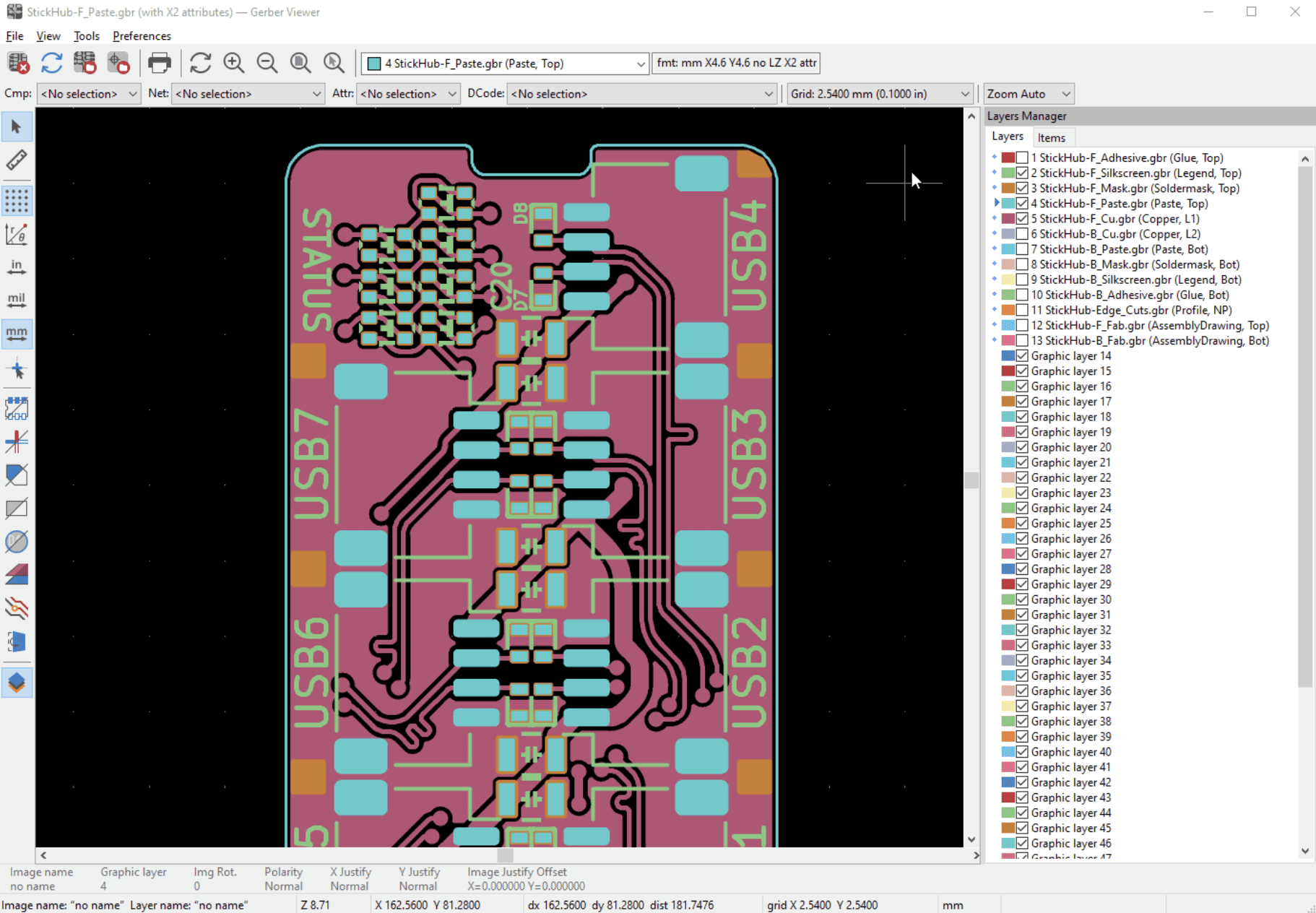
Use Gerber Viewer to open the newly exported Gerber and drill files together. With Computer Use, Claude can navigate layers and help inspect J1’s pads, mask openings, surrounding copper, and board-edge relationship.
Ask it to report which files are loaded and any visible misalignment or missing layers. A screenshot of the PCB Editor is not evidence that the exported package contains those same features.
Finally, request a manifest listing source revision, export settings, filenames, and unresolved questions. Keep that manifest with the package. Approve external sharing separately, after reviewing the outputs and completing any required engineering or manufacturer checks.
Source: KiCad Documentation Contributors
Keep Larger KiCad Workflows Responsive With Vagon
Your PCB workflow should not depend on whether your laptop can comfortably handle the next project. As designs grow, detailed 3D models, larger boards, and multiple review tools can put more pressure on your workstation.
Vagon Cloud Computer gives you a remote Windows desktop with selectable CPU, RAM, and GPU configurations, accessible from your existing device. You can change performance configurations while keeping the same cloud computer and files, making it practical to match resources to different workloads.
For KiCad, choose capacity around the actual bottleneck. CPU performance and available memory matter for computational tasks and larger projects; graphics resources are relevant to interactive visualization. A more powerful GPU should not be treated as an automatic accelerator for ERC or DRC.
The workspace also gives you somewhere to install KiCad, Claude, and your chosen MCP connector together. Keeping project files, libraries, and connector dependencies in that environment can reduce the path mismatches that arise when tools run on separate machines. You still need to configure and verify the integration yourself.
If you intend to use Computer Use, test it inside the supported Claude environment on the cloud desktop. Controlling a local browser displaying Vagon is not equivalent to direct access to KiCad’s windows.
A simple sensor board may run perfectly well locally. When project complexity or workstation limitations start slowing your review, Vagon offers a way to access additional resources without replacing your everyday computer.
FAQs
Can Claude edit KiCad schematics through MCP?
Some community connectors expose schematic editing tools, but the implementation matters. KiCad 9 and 10’s official IPC API covers the PCB Editor, not live schematic editing. A connector may instead modify schematic files directly. Check its supported operations, save behavior, and version requirements before authorizing changes. Reopen and validate modified files in KiCad.
Do I need Computer Use if I already have an MCP connector?
Not necessarily. Structured queries, supported edits, rule checks, and exports may be available without screen control. Computer Use becomes useful when a task requires navigating dialogs or examining visual context. Neither method substitutes for the other automatically. Choose the access method that provides reliable evidence for the specific task.
Can Claude review a KiCad project without opening the editor?
Yes, when its environment provides file access or suitable tools. Claude can analyze saved project information and interpret CLI reports without a running editor. However, that review cannot capture unsaved changes. Screenshots alone also provide incomplete connectivity information, so supply the underlying project files when detailed analysis is required.
Can Claude automatically route an entire PCB?
Some connectors integrate routing tools such as Freerouting. That does not establish that the result meets your electrical, mechanical, or manufacturing requirements. Routing depends on placement and constraints, while issues such as return paths or sensitive signal routing require additional judgment. Begin with a recoverable copy and review the resulting copper before accepting it.
Does passing ERC and DRC mean the board is ready to manufacture?
No. These checks evaluate modeled connections and geometry against configured rules. They do not guarantee correct component selection, acceptable operating conditions, mechanical fit, or circuit behavior. Review datasheets, manufacturing outputs, and assembly requirements separately. Designs with significant safety implications require qualified engineering review beyond AI assistance.
Can I run Claude and KiCad together on a cloud computer?
A compatible cloud desktop can host both applications and the connector dependencies. You must still verify installation, project paths, permissions, and any live editor connection. Computer Use additionally depends on Claude’s supported environment and access requirements. Test the workflow on a project copy before relying on it for production changes.
A sensor board can pass its rule checks and still arrive with a connector facing the wrong direction. The schematic may be consistent, the copper clearances acceptable, and the manufacturing files complete, yet the selected footprint might not match the part you ordered. Using Claude with KiCad is most useful when it helps you investigate those gaps, not just generate a circuit that looks plausible.
There are two complementary ways to connect that assistance to your project. A community-built MCP connector can expose design information and supported editing operations to Claude. Depending on its implementation, those tools may read saved files, invoke KiCad utilities, or interact with the running PCB Editor. Claude’s Computer Use provides a different route: working through the application interface to inspect dialogs, navigate findings, and perform visual checks.
Neither approach gives Claude unrestricted understanding of your hardware. Access depends on your KiCad version, connector, Claude environment, and permissions. A successful operation also needs verification against the correct project state.
This guide follows an existing two-layer sensor board through review, a controlled placement change, and manufacturing output checks. The goal is practical assistance with traceable changes, while you retain responsibility for electrical decisions and production approval.
Source: KiCad Documentation Contributors
Choose the Right Kind of Access for Each KiCad Task
Before connecting Claude, decide what the task actually requires. Reading a component list, moving a footprint, and inspecting a connector in the 3D Viewer are different operations. They do not necessarily need the same access method.
Access method | Best suited to | Main limitation |
|---|---|---|
Saved files and CLI | Project analysis, rule checks, manufacturing exports | May not reflect unsaved editor changes |
MCP connector | Structured queries and supported design operations | Capabilities depend on the connector and backend |
Computer Use | Dialogs, visual inspection, and interface interactions | Screen access does not provide complete design data |
These methods can overlap. An MCP server might invoke the KiCad CLI to run DRC, parse schematic files to inspect connections, and use an API for PCB operations. MCP describes how Claude accesses tools, not how those tools access KiCad.
That distinction matters for version compatibility. The official KiCad IPC API supports the running PCB Editor in KiCad 9 and 10. A connector that edits schematics in those versions must use another mechanism. Its schematic capabilities should not be assumed from its PCB capabilities.
For our sensor board, structured tools are useful for identifying references, nets, and footprint assignments. Computer Use can then help navigate the corresponding objects and examine their visual context.
Before either route makes changes, establish which project and revision Claude is inspecting. Ask whether each tool reads the saved file, the running editor, or its own in-memory copy. Otherwise, a successful check could describe an older board rather than the one visible on your screen.
Connect Claude to KiCad Without Mixing Backends
For a concrete starting point, the community-built KiCAD-MCP-Server provides a Python and TypeScript bridge between an MCP client and KiCad. It is not a native Claude integration or an official KiCad feature. Review its installation requirements and permissions before giving it access to a working design.
Install the connector and check its Python environment
The repository’s quick start specifies KiCad 9.0 or later, Node.js 18 or later, and Python 3.11 or later. It recommends the stable branch rather than unreleased changes on main:
These commands download and build the server, but they do not complete every platform-specific dependency step.
The important Python requirement is access to KiCad’s pcbnew module. An unrelated Python installation may run normally while failing to import it. Follow the connector’s platform guide for dependency installation, interpreter selection, and library paths. Windows and macOS installations can use KiCad’s bundled Python; Linux configuration depends on the installed packages.
Use paths detected on your machine. Do not copy a KiCad 9 library path into a KiCad 10 installation simply because it appears in an example.
Register the server with Claude
The connector’s Claude Desktop configuration launches the built server through Node. Its basic structure looks like this:
{
  "mcpServers": {
    "kicad": {
      "command": "node",
      "args": [
        "/ABSOLUTE/PATH/KiCAD-MCP-Server/dist/index.js"
      ]
This is a template, not a complete cross-platform configuration. Replace the placeholders and include any additional environment settings required by your installation. Merge the entry with existing MCP settings instead of replacing other servers.
After restarting Claude Desktop, check that the server connects and exposes tools. If it fails, inspect the connection logs before asking Claude to troubleshoot through repeated design operations.
Start with a read-only project check
Use a copy of the sensor-board project for the first test:
Identify the KiCad project you can access. Report its project path, board file, schematic files, and component references. Explain whether the information comes from saved files or a running editor. Do not modify or save anything.
Compare the response with KiCad before proceeding. A connected server pointing to the wrong project is still the wrong setup.
Finally, treat live access as a separate capability. This connector documents its IPC-based UI integration as experimental. File-based tools do not necessarily require an open editor; live tools do. Confirm the backend and synchronization behavior of the specific operation you intend to use before enabling edits.
Review the Circuit Before Moving Components
Start with a question about the design, not an instruction to rearrange it. For our sensor board, the first question is whether the external connector connects the intended signals to the correct physical pins.
Ask Claude to extract the connector’s reference, symbol pin numbers, connected nets, assigned footprint, and manufacturer part number. If the connector cannot expose one of those details, supply the relevant file or inspect it in KiCad. Missing information should remain an explicit uncertainty.
Source: KiCad Documentation Contributors
Compare the symbol, footprint, and actual part
KiCad matches symbol pins to footprint pads by their numbers. A net connected to symbol pin 1 therefore needs to reach the appropriately numbered footprint pad. But that correspondence alone does not establish that the footprint represents your purchased connector.
Compare three sources: the schematic symbol, the assigned footprint, and the manufacturer’s datasheet for the exact part. Check pad numbering, pitch, mounting style, and the viewing direction used in the mechanical drawing. A mating-face drawing and a board-side view can make the same connector appear reversed.
A focused request would be:
Review J1 without changing the project. Compare its symbol pin numbers, connected nets, and footprint pad numbers against the supplied manufacturer datasheet. Identify the drawing’s viewing direction. Separate confirmed matches, suspected mismatches, and details you cannot verify.
Require datasheet page references for conclusions based on the document. If the part number is incomplete or the drawing is ambiguous, Claude should ask for clarification rather than choose an orientation.
Extend the review to the surrounding circuit
Once J1 is understood, examine the paths connected to it. For a sensor interface, that could include the supply rail, ground connection, signal lines, and any pull-up or protection components. Ask Claude to distinguish what the project explicitly records from what it infers about the intended operation.
Source: KiCad Documentation Contributors
A compact findings table keeps this review actionable:
Item | Evidence to compare | Required outcome |
|---|---|---|
Connector mapping | Nets, pin numbers, pad numbers, datasheet | Confirmed mapping or unresolved discrepancy |
Footprint selection | Exact package, pitch, mounting dimensions | Compatibility evidence |
Component identity | Value, part number, BOM fields | Missing or inconsistent information flagged |
Run ERC as a baseline, but do not turn this review into automatic warning suppression. Record each finding with its reference and supporting evidence.
The result should be a prioritized review, not an edited board. Resolve identity and connectivity questions before approving a placement change, because moving the wrong footprint more neatly does not fix the underlying design.
Make One PCB Change You Can Verify
With J1’s identity and pin mapping confirmed, the next task is a bounded placement change. Avoid asking Claude to “optimize the board.” That instruction leaves too much room to move components, alter routing, or change constraints without a clear acceptance test.
Instead, identify the footprint by reference and, where available, its unique identifier. Ask Claude to report its current position, rotation, board side, and lock status before proposing a change. Coordinates need units and a stated origin; rotation needs a clear absolute target rather than an ambiguous instruction such as “turn it around.”
Source: KiCad Documentation Contributors
Define the change before approving it
For our sensor board, the objective is to orient J1 toward the intended cable-entry edge without changing its electrical mapping. Claude should first inspect the surrounding area and explain whether the proposed placement would affect nearby components or existing copper.
A suitable request is:
Inspect J1 and propose a placement that faces the approved cable-entry edge. Report its current and proposed coordinates, rotation, board side, and expected routing impact. Preserve the footprint assignment, pad net assignments, board outline, mounting holes, and other components. Do not apply the change until I approve the exact placement.
Before approval, save a recoverable project copy. Establish which application or tool owns the editable state so that a later save from another instance does not overwrite the result. If J1 is locked, ask why before authorizing an override.
Once the proposal is acceptable, approve only that operation. If the connector cannot perform it reliably, stop or explicitly switch to an interface-based method.
Treat placement and routing as separate operations
A footprint can retain its pad net assignments while losing physical copper connections after movement. A successful position update therefore does not prove that the board remains connected.
KiCad’s interactive routing has its own behavior and settings. Do not assume a connector’s coordinate-editing tool behaves like dragging through the router. Ask Claude to report disconnected pads and affected tracks rather than silently launching a broader rerouting operation.
After the change, request a compact comparison:
Property | Verification |
|---|---|
Position and rotation | Match the approved target |
Footprint and board side | Remain unchanged |
Pad net assignments | Match the original mapping |
Surrounding objects | No unintended modifications |
Copper connections | Inspected for required repairs |
Read these properties back from the updated state instead of relying only on the tool’s success message. Inspect J1 in KiCad, then run the appropriate checks on the synchronized, saved revision. Any routing repair should become a separate, explicitly scoped task.
Let Computer Use Handle the Checks That Need a Screen
MCP tools can report coordinates, net assignments, and rule violations, but some questions are easier to investigate inside KiCad. Which way does the connector opening face? Which objects surround a clearance marker? Does the footprint preview match the package drawing?
Claude’s Computer Use can help navigate those checks in a supported desktop environment with your permission. Enable the feature in the appropriate Claude application and approve the required access. Connecting an MCP server alone does not grant screen control.
The following are practical workflows to try, not guarantees that Claude will interpret every KiCad view correctly. Begin with inspection-only instructions and keep project-changing actions separately authorized.
Cross-probe the connector instead of searching twice
KiCad supports cross-probing between schematic symbols and PCB footprints, including corresponding pins and pads. Claude can use this interface to navigate from J1 in the schematic to its physical representation.
Ask it to select the relevant pin, inspect the corresponding pad, and report the visible net and numbering. This helps connect the earlier structured review to the actual objects on screen.
Select J1 in the schematic and locate its corresponding PCB footprint. Inspect pin 1 and its matching pad. Report what the interface shows without moving objects or changing properties.
If cross-probing is disabled or the association is missing, Claude should report that limitation rather than select a visually similar footprint.
Compare footprint candidates without assigning them
When a footprint choice remains uncertain, Computer Use can help open the assignment interface, filter candidates, and inspect previews. For a connector, compare pitch, pad count, mounting holes, and body orientation with the exact manufacturer drawing.
Request a shortlist with reasons, not an immediate replacement. Library names and attractive previews are insufficient evidence of compatibility. Applying a different footprint also requires checking how its pad numbering affects the existing design.
This workflow is especially useful when the connector exposes a footprint identifier but does not provide enough geometry for a confident comparison.
Source: KiCad Documentation Contributors
Navigate a DRC finding in its physical context
A report may identify two colliding items, while the board view makes their relationship clearer. Claude can open the checker, select a finding, zoom to its location, and inspect the surrounding copper and components.
Ask it to describe the reported violation and visible context separately. It should not change rule severity, exclude the finding, or adjust routing simply to remove the marker. If the view is ambiguous, request another zoom level or inspect the object properties.
Source: KiCad Documentation Contributors
Inspect connector orientation in the 3D Viewer
The 3D Viewer provides another perspective on J1’s approved placement. Claude can navigate around the board and check whether the displayed connector faces the intended edge or appears obstructed by neighboring components.
Treat this as visual evidence, not a mechanical clearance certificate. Models can be missing, incorrectly positioned, or different from the purchased part. Cable access also cannot be confirmed if the cable and enclosure are absent.
The useful outcome is a documented observation or unresolved question that you can verify against dimensions and hardware.
Source: KiCad Documentation Contributors
Read ERC and DRC as Findings, Not Certificates
After changing J1, the useful question is not simply whether the error count went down. It is whether the approved change introduced new problems, resolved the intended issue, or left existing findings unchanged.
Save and synchronize the project before running file-based checks. Then use the KiCad CLI to generate reports Claude can compare:
Replace the example filenames with your project’s paths. Keep the baseline reports separately rather than overwriting them. Record the KiCad version and use equivalent checking options for both runs.
Ask Claude to compare individual findings, not just totals:
Compare the baseline and updated ERC and DRC reports. Separate new, resolved, and unchanged findings. Identify affected references and locations where available. Do not change rules, exclusions, or project files.
An unchanged total can hide one resolved violation and one newly introduced violation. Likewise, fewer findings may reflect altered settings rather than an improved design.
Source: KiCad Documentation Contributors
Check the conditions behind the report
For PCB checks, confirm that copper zones have been refilled appropriately. KiCad 10’s CLI provides --refill-zones; saving the resulting board is a separate option. Where applicable, --schematic-parity also checks agreement between the PCB and schematic. Choose these options deliberately and preserve the same conditions when comparing revisions.
Review warnings and exclusions alongside errors. Do not authorize Claude to reduce clearance requirements, change pin types, or suppress findings merely to produce a clean report.
ERC and DRC evaluate modeled information against configured rules. They do not establish that the selected connector fits, that a component operates within its ratings, or that the circuit behaves correctly. A clean result is supporting evidence for review, not permission to manufacture without further verification.
Build a Manufacturing Package From One Saved Revision
Once the approved changes and checks are complete, freeze the project revision used for export. Do not generate Gerbers from yesterday’s board and combine them with today’s BOM. Give the package a revision-specific folder and keep subsequent exports separate.
Claude can coordinate supported connector tools or manufacturing exports through the CLI. Before execution, specify the source files, output directory, required layers, and manufacturer’s formatting requirements. File generation should not include uploading the design or placing an order.
Source: KiCad Documentation Contributors
For our two-layer sensor board, review the package by purpose:
Output | What to verify |
|---|---|
Gerber files | Required copper, solder mask, silkscreen, and board outline |
Drill files | Plated and non-plated holes, units, and alignment |
BOM | References, quantities, exact part numbers, and DNP handling |
Placement files | Included components, units, origin, board side, and rotation convention |
Assembly providers may require different BOM columns or placement conventions. Ask Claude to compare the generated files against your provider’s requirements rather than assuming a generic export is acceptable.
Inspect the exported files, not just the project
Use Gerber Viewer to open the newly exported Gerber and drill files together. With Computer Use, Claude can navigate layers and help inspect J1’s pads, mask openings, surrounding copper, and board-edge relationship.
Ask it to report which files are loaded and any visible misalignment or missing layers. A screenshot of the PCB Editor is not evidence that the exported package contains those same features.
Finally, request a manifest listing source revision, export settings, filenames, and unresolved questions. Keep that manifest with the package. Approve external sharing separately, after reviewing the outputs and completing any required engineering or manufacturer checks.
Source: KiCad Documentation Contributors
Keep Larger KiCad Workflows Responsive With Vagon
Your PCB workflow should not depend on whether your laptop can comfortably handle the next project. As designs grow, detailed 3D models, larger boards, and multiple review tools can put more pressure on your workstation.
Vagon Cloud Computer gives you a remote Windows desktop with selectable CPU, RAM, and GPU configurations, accessible from your existing device. You can change performance configurations while keeping the same cloud computer and files, making it practical to match resources to different workloads.
For KiCad, choose capacity around the actual bottleneck. CPU performance and available memory matter for computational tasks and larger projects; graphics resources are relevant to interactive visualization. A more powerful GPU should not be treated as an automatic accelerator for ERC or DRC.
The workspace also gives you somewhere to install KiCad, Claude, and your chosen MCP connector together. Keeping project files, libraries, and connector dependencies in that environment can reduce the path mismatches that arise when tools run on separate machines. You still need to configure and verify the integration yourself.
If you intend to use Computer Use, test it inside the supported Claude environment on the cloud desktop. Controlling a local browser displaying Vagon is not equivalent to direct access to KiCad’s windows.
A simple sensor board may run perfectly well locally. When project complexity or workstation limitations start slowing your review, Vagon offers a way to access additional resources without replacing your everyday computer.
FAQs
Can Claude edit KiCad schematics through MCP?
Some community connectors expose schematic editing tools, but the implementation matters. KiCad 9 and 10’s official IPC API covers the PCB Editor, not live schematic editing. A connector may instead modify schematic files directly. Check its supported operations, save behavior, and version requirements before authorizing changes. Reopen and validate modified files in KiCad.
Do I need Computer Use if I already have an MCP connector?
Not necessarily. Structured queries, supported edits, rule checks, and exports may be available without screen control. Computer Use becomes useful when a task requires navigating dialogs or examining visual context. Neither method substitutes for the other automatically. Choose the access method that provides reliable evidence for the specific task.
Can Claude review a KiCad project without opening the editor?
Yes, when its environment provides file access or suitable tools. Claude can analyze saved project information and interpret CLI reports without a running editor. However, that review cannot capture unsaved changes. Screenshots alone also provide incomplete connectivity information, so supply the underlying project files when detailed analysis is required.
Can Claude automatically route an entire PCB?
Some connectors integrate routing tools such as Freerouting. That does not establish that the result meets your electrical, mechanical, or manufacturing requirements. Routing depends on placement and constraints, while issues such as return paths or sensitive signal routing require additional judgment. Begin with a recoverable copy and review the resulting copper before accepting it.
Does passing ERC and DRC mean the board is ready to manufacture?
No. These checks evaluate modeled connections and geometry against configured rules. They do not guarantee correct component selection, acceptable operating conditions, mechanical fit, or circuit behavior. Review datasheets, manufacturing outputs, and assembly requirements separately. Designs with significant safety implications require qualified engineering review beyond AI assistance.
Can I run Claude and KiCad together on a cloud computer?
A compatible cloud desktop can host both applications and the connector dependencies. You must still verify installation, project paths, permissions, and any live editor connection. Computer Use additionally depends on Claude’s supported environment and access requirements. Test the workflow on a project copy before relying on it for production changes.
Get Beyond Your Computer Performance
Run applications on your cloud computer with the latest generation hardware. No more crashes or lags.

Trial includes 1 hour usage + 7 days of storage.
Summarize with AI

Ready to focus on your creativity?
Vagon gives you the ability to create & render projects, collaborate, and stream applications with the power of the best hardware.

Vagon Blog
Run heavy applications on any device with
your personal computer on the cloud.
San Francisco, California
Solutions
Vagon Teams
Vagon Streams
Use Cases
Resources
Vagon Blog
How to Use KiCad With Claude: MCP & Computer Use Guide Meta
How to Use FreeCAD With Codex: MCP & Computer Use
How to Use FreeCAD With Claude: MCP & Computer Use
How to Use 3ds Max With Codex: MCP & Computer Use
How to Use Houdini With Claude: MCP & Computer Use
How to Use Cinema 4D With Claude: MCP & Computer Use
How to Use 3ds Max With Claude: MCP & Computer Use
How to Use DaVinci Resolve With Claude: MCP & Computer Use
How to Use Godot With Claude: MCP & Computer Use
Vagon Blog
Run heavy applications on any device with
your personal computer on the cloud.
San Francisco, California
Solutions
Vagon Teams
Vagon Streams
Use Cases
Resources
Vagon Blog
How to Use KiCad With Claude: MCP & Computer Use Guide Meta
How to Use FreeCAD With Codex: MCP & Computer Use
How to Use FreeCAD With Claude: MCP & Computer Use
How to Use 3ds Max With Codex: MCP & Computer Use
How to Use Houdini With Claude: MCP & Computer Use
How to Use Cinema 4D With Claude: MCP & Computer Use
How to Use 3ds Max With Claude: MCP & Computer Use
How to Use DaVinci Resolve With Claude: MCP & Computer Use
How to Use Godot With Claude: MCP & Computer Use
Vagon Blog
Run heavy applications on any device with
your personal computer on the cloud.
San Francisco, California
Solutions
Vagon Teams
Vagon Streams
Use Cases
Resources
Vagon Blog